Team6 · August 12, 2026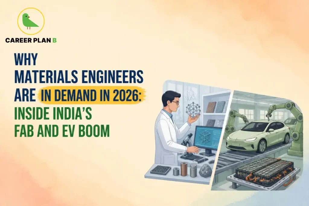
Introduction
India’s semiconductor sector alone is projected to generate demand for close to a million jobs by FY 2026-27, and materials engineering appears explicitly on the list of specialized skills this industry urgently needs. Understanding why materials engineers are in demand in 2026 requires looking closely at what’s actually driving this surge, since it isn’t confined to one single sector or a temporary hiring spike. Many students assume semiconductor and EV hiring booms are reserved purely for electronics or mechanical engineers, completely missing how specifically materials engineers get named across these industry reports. This blog breaks down exactly why 2026 marks a genuine turning point for this specialization, which sectors are driving it, and what it means for your career.
Why 2026 Is a Genuine Inflection Point for Materials Engineers
India Semiconductor Mission 2.0’s Explicit Focus on Materials
The clearest signal comes directly from government policy itself. According to the Press Information Bureau, India Semiconductor Mission 2.0, announced in the Union Budget 2026-27, will explicitly focus on producing semiconductor equipment and materials domestically, alongside designing full-stack Indian intellectual property and fortifying supply chains. The Finance Ministry has since cleared a ₹1.25 lakh crore outlay for this mission, considerably higher than the ₹76,000 crore allocated to ISM 1.0, signalling genuinely serious, sustained commitment rather than a one-time announcement. Consequently, India Semiconductor Mission 2.0 isn’t just about building fabs; it’s specifically targeting the materials, chemicals, and gases that make chip manufacturing possible domestically, a shift that puts materials engineers directly in the policy spotlight.
The Scale of India’s Semiconductor Hiring Push
Beyond policy language, the actual hiring numbers reinforce this urgency considerably. Industry reports project the semiconductor sector could generate demand for over a million jobs by FY 2026-27, spanning fabrication, ATMP, chip design, and supply chain functions, with materials engineering specifically named as one of the core specialist categories needed to build this talent pipeline. Additionally, 12 semiconductor manufacturing projects have already been approved with an investment pipeline of about ₹1.64 lakh crore, including fabrication units and packaging facilities that all require materials expertise to operate. Therefore, semiconductor jobs India-wide are scaling at a pace that genuinely outstrips the current supply of specialized talent.
Where Materials Engineers Fit Into Semiconductor Fabs
Is this demand real and specific, or just generic engineering hiring dressed up in exciting language? The evidence points toward a genuinely specific need. Industry analysis identifies chemical and materials engineers as essential specifically for etching, gas deployment, and silicon wafer purification, processes that sit at the technical core of how a semiconductor fab actually operates. Fab process engineering roles covering lithography, etch, and deposition are opening at scale as new plants ramp up production, alongside quality and reliability engineering positions that depend heavily on materials science expertise. This isn’t a vague, catch-all mention; it’s a precise technical requirement tied to specific manufacturing steps that only materials-trained engineers can handle competently.
Beyond Semiconductors: Other Sectors Driving This 2026 Demand
EV and Battery Materials: A Parallel Growth Story
Semiconductors aren’t the only sector pulling materials engineers into high demand right now. Automotive manufacturing, driven heavily by the push toward electric vehicles, increasingly requires materials specialists to research and develop stronger, lighter components and battery materials that improve both performance and sustainability. This EV materials engineering demand runs parallel to India’s broader battery manufacturing push, since developing better battery chemistries and lighter vehicle components both depend fundamentally on materials science expertise rather than purely mechanical or electrical engineering knowledge alone.
Aerospace and Defence’s Advanced Materials Needs
Aerospace and defence represent another consistently strong driver of this demand, since these sectors specifically require expertise in advanced materials like lightweight composites and heat-resistant alloys that enhance aircraft and spacecraft performance. Graduates entering this space typically work on developing and testing these specialized materials against strict industry standards, work that connects directly to India’s broader defence manufacturing expansion under Atmanirbhar Bharat. Consequently, materials science jobs in the 2026-wide span are considerably more than one industry, reflecting genuine, structural demand across India’s most strategically important manufacturing sectors simultaneously.
Is this demand backed by real numbers or just industry hype?
So is this genuinely reliable demand, or could it fade quickly like some hyped-up tech trends do? The honest picture includes both real opportunity and real risk. The semiconductor workforce specifically is expected to grow from 345,000 to 460,000 professionals by 2030, yet nearly 58 per cent of new jobs, including 80 per cent of technical roles, may remain unfilled due to low advanced-engineering graduation rates in specialized areas. This substantial gap actually strengthens the case for materials engineers entering the field now, since genuine talent scarcity, rather than oversupply, defines this specific moment. However, it also means execution challenges are real, and students should approach this opportunity with genuine skill-building rather than assuming demand alone guarantees an easy entry.
Have Any Doubts?
Skills Materials Engineers Need to Capture This 2026 Opportunity
Cleanroom and Fabrication-Specific Technical Skills
Succeeding in this space requires more than general materials science knowledge; it demands specific familiarity with cleanroom operations, fabrication processes, and semiconductor equipment handling. Employers increasingly prioritize candidates who understand these fabrication-specific technical demands directly, rather than relying purely on theoretical materials science coursework covered in a standard undergraduate curriculum.
Why Job-Readiness Matters More Than the Degree Alone
Industry analysis makes a genuinely important point here: while India produces roughly 600,000 electronics and allied engineering graduates annually, only a small fraction are actually prepared for the realities of fabrication, ATMP operations, or advanced materials roles. This means job-readiness, built through hands-on projects, internships, and exposure to real fabrication tools, matters considerably more for landing these roles than academic credentials alone. Building this practical exposure early genuinely strengthens your materials engineering scope and competitiveness within this fast-growing but skills-constrained market.
Career Roles and Growth Path
| Career Stage | Typical Role | Where You Might Work |
|---|---|---|
| Entry-Level | Junior Process/Materials Engineer | Semiconductor fabs, ATMP facilities, EV battery manufacturers |
| Mid-Level | Semiconductor Materials Engineer / Quality Engineer | Tata Electronics, Micron, defence and aerospace manufacturers |
| Senior-Level | Materials R&D Lead / Fab Process Manager | Large semiconductor and advanced manufacturing companies |
Senior semiconductor engineers in India currently earn up to $38,390 annually, with top-tier professionals commanding compensation as high as $90,233, reflecting a 25 to 35 percent premium over broader IT and software roles. Given this pay premium and the persistent talent shortage across technical roles, a semiconductor materials engineer career path offers genuinely strong compensation growth for those who build the right specialized skills early.
How Career Plan B Helps
Career Plan B helps students make informed career decisions in emerging technology-driven engineering fields through personalized guidance, assessments, and structured career planning. Choosing a specialization like materials engineering requires understanding your interests, technical abilities, industry trends, and long-term career goals.</p>
<p>Personalized Career Counselling: Provides expert guidance to help students explore opportunities in materials engineering, semiconductor manufacturing, EV battery technology, aerospace materials, and advanced manufacturing based on their interests and career aspirations.<p>Psychometric & Career Assessment Tests: Helps identify individual strengths, personality traits, technical preferences, and suitable career paths across areas like materials science, semiconductor technologies, renewable energy, research, and industrial innovation.<p>Career Roadmapping: Creates a step-by-step career plan covering degree selection, specialization options, skill development, internships, certifications, higher education, and industry preparation for high-growth fields such as semiconductor materials engineering and EV materials engineering.<p>Admission & Academic Profile Guidance: Helps students choose the right engineering courses, colleges, and specialization paths while improving their academic profile for careers in advanced materials, semiconductor manufacturing, battery technology, and research-driven industr
ies.
Get In Touch With Us
Frequently Asked Questions
Q1. Why are materials engineers specifically in demand for semiconductor jobs?
Semiconductor fabs need materials expertise specifically for etching, gas deployment, and wafer purification, processes that sit at the core of chip manufacturing.
Q2. Is this demand only in semiconductors or other sectors too?
No, EV and battery manufacturing, along with aerospace and defence, are also driving strong parallel demand for materials-engineering expertise.
Q3. Do I need a master’s degree to get into semiconductor materials roles?
Not always a B.Tech with demonstrable, job-ready skills and hands-on project experience can land many manufacturing and process-focused roles without a postgraduate degree.
Q4. Which cities have the most materials engineering opportunities right now?
Bengaluru, Hyderabad, and Noida lead in design-focused roles, while Dholera, Greater Noida, and Prayagraj are emerging hubs for fabrication and materials-related manufacturing roles.
Q5. Is this a genuine long-term trend or a short-term hiring spike?
It’s a genuine, structural trend, backed by a ₹1.25 lakh crore government commitment through ISM 2.0 and persistent talent shortages projected to continue through 2030.
Conclusion
Understanding why Materials Engineers Are in Demand in 2026 shows that this is more than a temporary hiring trend. It reflects a long-term shift driven by government investment and growing demand across semiconductor, EV, and defence manufacturing. As the India Semiconductor Mission 2.0 expands domestic materials and equipment production, EV and aerospace industries are also increasing manufacturing capacity. Engineers who develop practical, fabrication-specific skills can expect strong long-term career opportunities. This creates a real opportunity for students who focus on industry-ready expertise instead of relying only on theoretical knowledge.
If you’re planning a career in this high-growth field, Career Plan B can help you build the right roadmap. With expert guidance and personalized planning, you can prepare for the skills and opportunities employers are actively looking for.